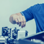
Applied Materials recently released their latest version of UVision, the system for inspecting semiconductor wafers. This system is based on a deep UV laser with various optical components that allow it to detect defects below the 10 nm scale.
As systems move to measure smaller sized features, they need smaller wavelength lasers (deeper into UV territory). UV lasers are not always the easiest to monitor, as many sensors do not detect those wavelengths, and they are prone to cause sensor damage as well.
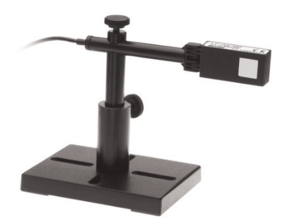
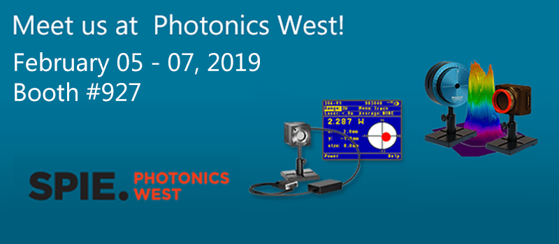
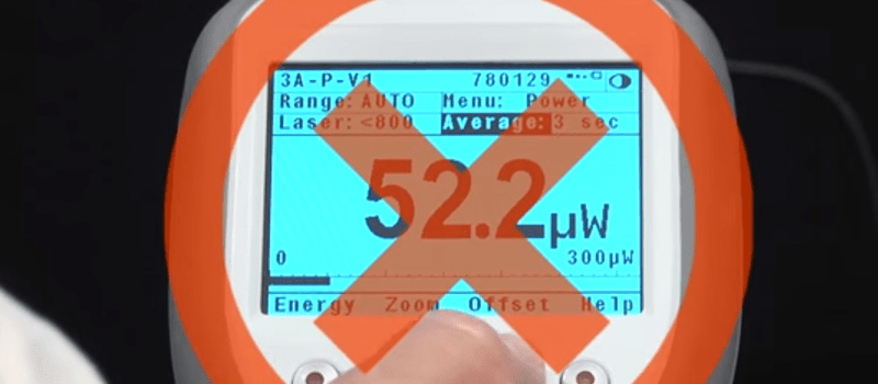
However, Ophir has several power and energy sensors made specifically to measure UV laser sources. (Of course, you should still be careful to keep the power and other parameters within specifications to protect your sensor from damage.)
At Applied Materials, these sensors are used for two purposes, both directly and indirectly.
Directly, they use several Ophir sensors to measure the power, power stability, and alignment of their DUV laser source. They also have some custom OEM sensors that are made tailored for their design and needs.
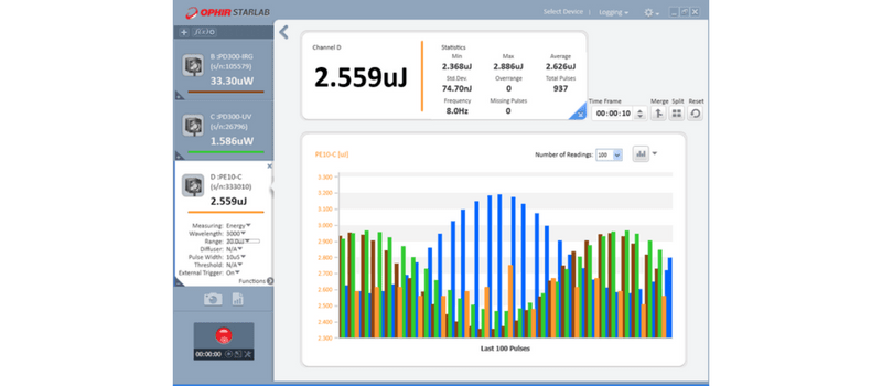
In an indirect way, they also use our sensors to measure UVision 8 optical components, to determine their reflectivity and transmittance.
Applied Materials needs highly accurate monitoring of their core and auxiliary components so their customers get the high level diagnostics they have come to expect from Applied Materials. For this, Applied Materials relies on Ophir.


Leave a Reply
Your email address will not be published. Required fields are marked *