Displays are all around us, from large TV screens to tiny displays inside AR/VR gear just in front of our eyes. Display technology has come a long way from the days of the bulky cathode ray tubes to transparent and flexible OLED displays utilizing light emitting organic molecules!
As new technologies take their place on stage, equipment suppliers follow carefully for trends and opportunities and the laser industry is no exception. In recent years, OLED and microLED are emerging as new technologies which are gradually replacing LCD (Liquid Crystal Display). In this post we look at the use of lasers in OLED and microLED display manufacturing
Brief technology overview
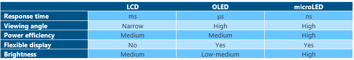
LCD is a transmissive technology, i.e. the function of the pixels is to block or pass light that is generated behind them. A voltage applied to a thin layer of liquid crystal held between two polarizers facilitates the on/off function.
OLED and microLED are emissive technologies where each pixel is a small light source. OLED pixels are based on light emitting organic molecules and microLED pixels are semiconductor LEDs. While OLED molecules are deposited directly on the display backplane, microLED chips are manufactured on a semiconduction wafer and need to be transferred.
While OLED is already widely adopted in the market, microLED technology still lags even though it offers several advantages. Presently, the key challenge in adopting microLED technology is the process of transferring the individual microLED pixels from the semiconductor wafer onto to the backplane of the final display product.
The following table shows several differences between these technologies.
Laser applications in OLED manufacturing
The process of making an OLED display is generally divided into three stages:
- Deposition and crystallization of amorphous silicon making the conductive wiring of the pixels
- Formation of pixels. Red, green, and blue emitting OLED molecules are deposited using vapor deposition or ink-jet printing
- Encapsulation and lift off.
- Encapsulation. OLED molecules are very sensitive to moisture. The display is encapsulated between thin layers of polymer or glass.
- Lift-off. OLED displays are manufactured on transparent polymer sheets. During the fabrication process, the display rests on a glass substate that supports it. When the display is ready, it is ‘peeled’ off the glass in what is called ‘lift off’
The following manufacturing step utilize lasers:
- Laser annealing – transforming of amorphous silicon into polycrystalline silicon. The energy imparted by the laser beam enable the silicon atoms to move around until they settle in a stable crystallized form.
- Laser liftoff – separating the OLED display from the glass substrate. The laser beam is formed into a narrow thin line that scans across the OLED display and is absorbed in the interface between the OLED display the glass interface and separates the two.
- Cutting and drilling of glass and polymer parts. Cutting and drilling with lasers is done by evaporating material rather than removing material, for example, using a drill. This allows processing thin and fragile materials without cracking them.
Laser application in microLED displays
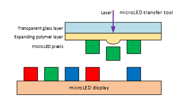
microLED pixels are manufactured in a ‘classic’ semiconductor process and need to be transferred onto the microLED display backplane. This is currently the most challenging step in microLED manufacturing. For a microLED TV screen, millions of micron sized microLED’s need to be transferred from the wafer onto the display backplane with high accuracy and speed. To add to the complexity, the microLEDs are much denser on the semiconductor wafer than they are on the display, making it impossible to transfer groups of microLEDs simultaneously.
Several companies are working on technologies for making this transfer step more efficient. One such company, Uniqarta, developed a technology that uses a rapidly moving laser beam to selectively release microLED chips from a polymer carrier onto the display backplane. The release of the microLED chip is achieved by local heating of the polymer carrier causing it to expand and create a ‘bump’ that pushes the microLED chip away.
Lasers for OLED and microLED manufacturing
Two major types of pulsed lasers, mainly in UV are used in OLED and microLED display manufacturing: Excimer lasers and solid state lasers.
Excimer lasers use a compound of a noble gas and a halogen, and they emit in the UV. Solid state lasers use diode lasers to pump a crystal, or a fiber doped with rate earth elements such as Neodymium which emit in the near IR. Additional crystals are used to double and triple the frequency. Additional components are used to control the pulse width down to fs. Several typical parameters of Excimer and solid state lasers are shown in the next table.
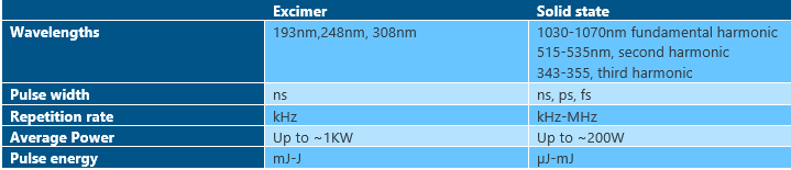
Excimer lasers can provide more power, however, this is not the only important parameter for increasing throughput. Pulse width also plays an important role. For a given pulse energy, as the pulse becomes shorter, the instantaneous power increases. As a result of the high instantaneous powers the material is vaporized before the heat can flow outside the intended work area and be wasted or worse, cause damage. This is sometimes referred to as ‘cold processing’ because one can cut through glass without heating it. Consequently, a process which requires 1000W using a ns laser may require much less power when using a fs laser.
While most applications require UV lasers, some use visible and IR laser:
- Heating solder for removing a defective microLED and soldering a new one in its place.
- Patterning of the fine metal mask in OLED
- Cutting of ultrathin glass.
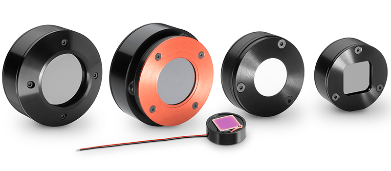
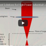
When it comes to measuring the power of such lasers, this becomes a real challenge. It is well known that selecting the right laser sensor depends on the average power, and power density in [KW/cm2]. For pulsed lasers, the energy density in [J/cm2] is also considered. However, short pulse lasers in the ps and fs range may have relatively low power and energy density but can still damage general purpose sensors due to the extremely high instantaneous power. This is especially true for UV lasers, where the photon energy is high, and photons can break molecular bonds more easily. The right sensor needs to be tailored to the application.


Leave a Reply
Your email address will not be published. Required fields are marked *