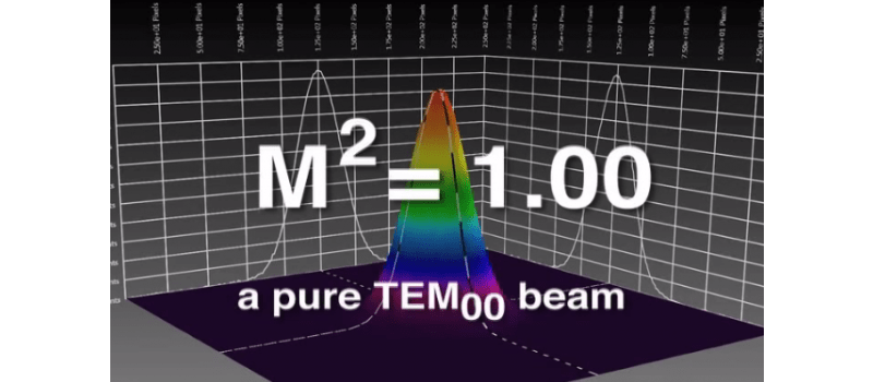
High-precision laser processing has become a vital manufacturing tool in industries ranging from automotive production to microelectronics fabrication. Achieving the full benefits of laser processing in these diverse applications almost always requires maintaining consistent source output. This means laser power and often the power distribution and beam profile, as well.
Camera-based systems are often used for making highly accurate laser beam profile and power distribution measurements. Originally these instruments utilized CCD (Charge-Coupled Device) sensors. But over the past few years, CCDs have largely disappeared from the market and been replaced by CMOS (Complementary Metal-Oxide-Semiconductor) detectors.
The Advantages of CMOS Sensors
CMOS sensors have achieved market dominance because they offer four key benefits over CCDs:
- Faster Readout: CMOS sensors can produce an image faster since each pixel is read simultaneously.
- Lower Cost: CMOS detectors are made using the same cost-effective semiconductor fabrication processes used for producing logic and memory chips.
- On-Chip Integration: CMOS sensors allow for integration of signal processing, amplifiers, and other functionality directly onto the sensor chip, enabling more compact and efficient designs.
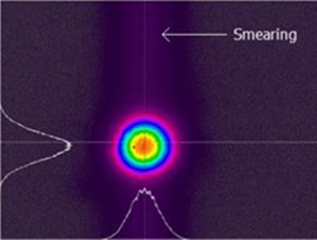
- No Smearing: Smearing – vertical streaks in the image – occurs in CCDs because some of the charge leaks into adjacent pixels as it is transferred down a vertical column during readout. But this effect is totally absent in CMOS sensors because each pixel is read independently without pixel-to-pixel charge transfer.
wavelengths
The Limitations of CMOS Imagers
But CMOS sensors are not without their limitations, particularly for measuring beam profiles of NIR lasers which are widely employed in industrial processing.
One challenge is “blooming” – this means a broadening of the laser beam on the detector which can produce inaccuracies in beam width and intensity distribution measurements.
Blooming occurs in the near infrared because these longer wavelengths are not strongly absorbed by silicon. This means IR light can penetrate all the way into the detector where internal reflections from the backside of the device can enter surrounding pixels. While CCDs are also made from silicon, their architecture makes it relatively easy to avoid blooming. But it’s harder to do this with CMOS sensors because the transistors for controlling each pixel are in a layer on top of the detectors. All this complex 3D structure and overlying circuitry make it more difficult to manage charge flow and implement effective blooming correction mechanisms within the detector.
Innovative Solutions from MKS
MKS engineers studied the behavior and characteristics of CMOS sensors extensively. What we learned enabled us to develop techniques for minimizing the blooming problem encountered when measuring the beam profiles of NIR lasers.
One innovation we employ is backside illumination. CMOS sensors are most typically used with frontside illumination. Here, the incident light passes through layers of transistors and wiring before reaching the photodiode structure. But this configuration reduces light collection efficiency, particularly for NIR wavelengths.
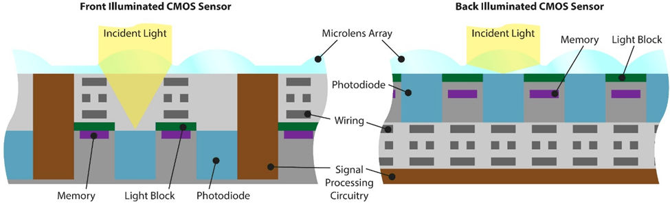
In backside illumination, incident light hits the photodiodes directly. This eliminates shading effects, improves sensitivity, and minimizes blooming. Further innovations include separating the signal processing and photosensitive layers, allowing each to be optimized independently. These advances dramatically enhance the accuracy of NIR beam profiling, while also improving overall performance and noise reduction.
Our most recently introduced beam profilers take advantage of backside illuminated CMOS sensors to deliver both high resolution and accuracy in a compact footprint. These include:
SP204S CMOS Beam Profiler: This beam profiler is based on a 1/1.8″ sensor (7.2 mm x 5.3 mm). The makes it capable of measuring both collimated beams as large as 5.6 mm diameter, as well as focused beams with spot sizes as small as 27 µm.
SP402S Large Format Beam Profiler: This beam profiler utilizes a much larger 1.1″ sensor format (12.3 mm x 12.3 mm). This enables it to characterize beams over a tremendous size range – from focused spots of 27 µm diameter to collimated or diverging beams up to 12 mm diameter.
Both of these cameras are supplied with our BeamGage software which provides a powerful but intuitive user interface as well as extensive analysis capabilities.
Measuring Small Diameter Beams
When measuring small NIR focal spots – those under about 100 µm diameter – additional steps beyond just backside illumination must be employed to achieve high absolute accuracy. To address this, MKS engineers developed a unique feature called “Blooming Correction.” This technique is used in our SP932U beam profiler to enable accurate measurements of focused beam diameters as small as 35 µm.
This blooming correction is actually a form of calibration. Specifically, during the product development process, we exhaustively tested the sensor used in the SP932U to determine ways to define the correct standard for all beam sizes and wavelengths. From this, we developed calibration methods and computational algorithms to correct the raw data produced by the sensor.
Specialized illumination patterns are projected onto the detector to map its blooming characteristics of each individual sensor. The resulting data is then used to fine-tune correction algorithms embedded in the profiler’s software. This ensures the beam profiler will deliver accurate measurements across various wavelengths, beam sizes, and intensities.
While the blooming correction enables the SP932U to measure everything from large to tightly focused NIR beams, it typically slows down the measurement rate and requires longer exposure times. This makes the SP204S or SP402S better choices if there is no need to measure NIR beams below 100 µm in diameter, or when working solely with visible or UV wavelength lasers where detector blooming isn’t an issue.
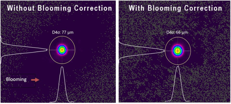
value of 77 µm, and with “Blooming Correction” it delivers the correct value of 66 µm.
Putting our Customers First
For many other manufacturers of beam profiling cameras, the switch from CCD to CMOS sensors was a simple replacement. But MKS recognized early on that a direct swap would compromise performance. Instead, our engineers took a step back and worked to ensure that every aspect of CMOS sensor technology was understood and then adapted to meet the specific demands of beam profiling. In particular, we paid attention to the measurement of NIR lasers because these have become so essential in many industries.
We followed this path because our focus isn’t just on delivering cutting-edge tools; it’s also on understanding how customers use them. This is what enables us to create products that consistently meet customers’ needs and expectations. By combining advanced sensor technology with this commitment to solving real-world problems, MKS continues to set the standard in laser beam analysis.


Leave a Reply
Your email address will not be published. Required fields are marked *