In the past few years, along with the world’s need for alternative energy, the solar panel production industry is expanding rapidly.
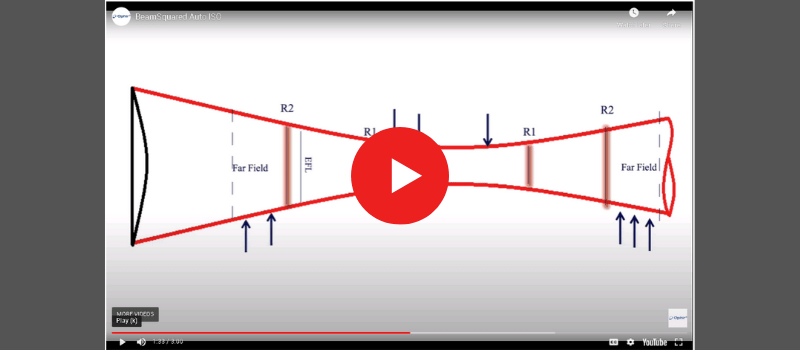
Many solar production lines use laser based methods to manufacture thin film silicon photovoltaic modules. In order to cut photovoltaic sheets precisely without overheating the photovoltaic material, it is necessary to use small diameter beams with high enough power density to cut smoothly and precisely. The laser commonly used for this purpose is a diode-pumped solid-state laser at a wavelength of either 355 nm, 532 nm or 1064 nm, focused down to about 30 mm.
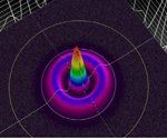
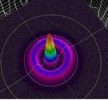
To ensure that the cuts of a photovoltaic sheet are uniform it is important to profile the beam. The question is what device should be used to profile these beams? Since these beams are powerful and have such small diameters the answer is not so clear.
CCD beam profilers would be difficult to use. Cameras have a hard time measuring beams with diameters which are less than 50μm. Furthermore, when profiling powerful beams with cameras, to prevent detector saturation, attenuation is required before the beam reaches the detector. Some times several stages of attenuation are needed in order to get a beam power which can be measured by a camera without damaging it. Attenuation schemes could be very complex, and could require a lot of space. Additionally, attenuation often causes distortion, which adds great uncertainty to the data measured.
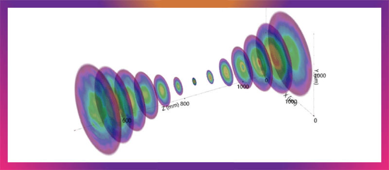
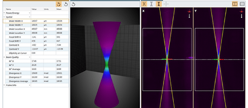
When using a scanning slit profiler, very small diameter beams can be measured with little or no need for attenuation schemes, the scanning slit acts as a physical attenuator. Photons NanoScan slit profiler is capable of directly measuring beams as small as several micro meters with little or no attenuation.
However, some of the beams used in the solar panel production facilities are pulsed beams. Although the NanoScan is capable of measuring pulsed beams, small diameter beams present a problem. Unless the repetition frequency of the pulses is very high, the nature of pulsed beam analysis limits the size that can accurately be measured. In addition, as the beam’s diameter decreases, the power or energy density increases dramatically, making damage to the profiler a possibility. Photon designed a profiler for the specific needs of the solar panel manufacturing process. They simply added a beam expander to the NanoScan Near-Field Profiler system. By expanding the beam before it reaches the profiler it reduces the energy/power density, and makes measurement of the beam possible .
For more specifications about this device you can read about it in the following link: Measuring Lasers Used in Photovoltaic Solar Panel Manufacturing
You might also like to read: How Laser Measurement Helps Keep Solar Cell Manufacturing Green
Share this:

Leave a Reply
Your email address will not be published. Required fields are marked *