Unveiling the Story Behind Moore’s Law
About fifty years ago, Gordon Moore, co-founder of Intel Corp, stated: “The number of transistors in an integrated circuit will double about every two years.” This prediction, famously known as “Moore’s Law,” has been a guiding principle in the semiconductor industry ever since, shaping long-term planning and research and development efforts. Today, the number of transistors in a microchip has surged from a mere few thousand to several billion, a staggering testament to technological advancement.
Consumer Demand: Driving Technological Innovation
Fueling this exponential growth is the insatiable demand from consumers for faster and more powerful electronic devices. From PCs and laptops to tablets and smartphones, our reliance on these gadgets continues to soar, pushing semiconductor technology to evolve at an unprecedented pace. This constant demand necessitates continual improvements in semiconductor manufacturing processes, particularly in photolithography, which plays a pivotal role in defining device patterns, including transistor position and size.
Pushing Boundaries: Introducing Extreme Ultraviolet Lithography (EUVL)
However, the limitations of current technologies are becoming increasingly apparent. Presently, pattern structures are predominantly produced using Deep Ultraviolet Lithography (DUVL), which utilizes 193nm laser radiation as a light source. While this technique has enabled remarkable achievements, it faces inherent constraints due to the wavelength of the light used. To overcome these limitations and sustain the trajectory set by Moore’s Law, innovative solutions are imperative.
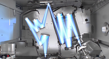
Enter Extreme Ultraviolet Lithography (EUVL), a groundbreaking advancement that leverages Extreme UV wavelengths to achieve unprecedented resolutions. With wavelengths close to X-ray, EUVL enables pattern structures to shrink to single nanometers, ushering in a new era of semiconductor manufacturing.
Ophir’s Role: Precision in Innovation, Driving Progress, Shaping the Future
Amidst these advancements, Ophir plays a crucial role in ensuring precision and control in the EUV process. Our advanced laser measurement technologies and engineering capabilities are integral to several critical steps of the EUV process. From real-time monitoring and control of CO2 laser power to precise beam positioning and safety measures, Ophir’s solutions uphold the highest standards of accuracy and reliability.
As we continue to push the boundaries of semiconductor technology, the road ahead is filled with both challenges and opportunities. The demands of projects like EUV lithography propel us to unprecedented levels of operation, setting new standards for precision and innovation. Despite the complexities and challenges, I am immensely proud and excited to be part of this remarkable journey, shaping the future of semiconductor technology.


Leave a Reply
Your email address will not be published. Required fields are marked *