In 1965, Intel’s Gordon Moore made a prediction about the future of technology that remained accurate far longer than even Moore himself expected. It has come be known as: “Moore’s Law.”
Moore observed that the number of components that fit on a chip (at minimum cost) had been doubling each year. He simply predicted that it would continue to do so. 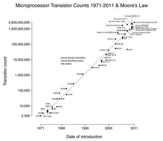
Processors supporting Moore’s Law; Author: Wgsimon
Over the course of the last 50 years, there have been multiple times when this exponential growth seemed to be approaching an inevitable slow-down.
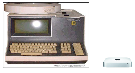
Every day, electronics get smaller. This trend allows for Moore’s law to continue, but more importantly, it means that we can accomplish more and more with less and less. For example, shown below is a Datapoint 2200 (one of the first PCs) and a Mac mini. The old computer, a Datapoint 2200 is dozens of times heavier and larger (the pictures below are approximately to scale), while the Mac’s processor speed and memory are orders of magnitude greater (about 6). On top of all that, the Datapoint would cost over $25,000 today (after inflation adjustment), while the Mac goes for $800.
Datapoint 2200 (1971); Author: Ecksemmess Mac mini (2011); Author: Wiki637
Gordon Moore observed this trend decades ago, but by-and-large it has continued well past anyone – even Moore – could have expected. Whenever the exponential seems to approach an insurmountable ceiling, a new technology is developed or some novel approach is designed that makes the impossible seem downright simple.
One example of a new technology extending Moore’s “prophecy” beyond the expected was Kanti Jain’s use of ultraviolet laser light to improve lithography in 1982. Shorter wavelengths mean smaller feature sizes, and currently a 193nm excimer laser is capable of producing chips with a 40nm dimension. (I know, this seems impossible, but clever methods are employed to actually create structures shorter than the wavelength of the laser itself.)
Once again, however, we’re starting to face an (seemingly) unavoidable obstacle. As chip designers attempt to create features smaller than 40nm, the natural next step is smaller wavelength UV lasers. If a 193nm can produce 40nm chips, why can’t a 13.5nm laser produce, say, 10nm chips? Perhaps it can, but there are proving to be several issues with using extreme UV (or EUV) lasers for this:
- EUV light is absorbed by almost everything, so the lithography needs to be done in a vacuum chamber, which greatly reduces productivity.
- EUV light is similarly highly absorbed by mirrors, so the original source needs to have much more power (around 20 times more) than is actually necessary to burn the photoresist.
- Furthermore, all that light absorbed in the mirrors and other components can lead to overheating.
Due to these issues, some are starting to look for some totally new method, referred to simply as “Next Generation Lithography (NGL).”
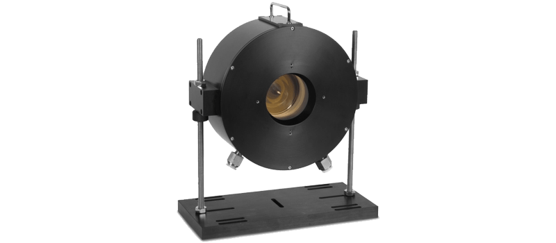
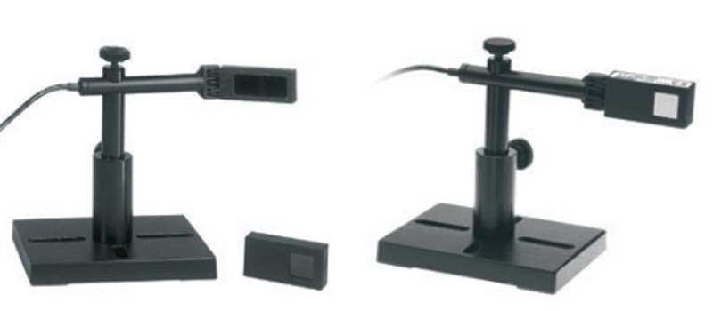
It remains to be seen which approach will be successful, but one thing is certain: in order to experiment with EUV lasers, one must have a power meter that can measure down to EUV. (Most sensors don’t.) Ophir, for example, generally states that sensors with a broadband coating measure accurately down to 190nm. However, the truth is that the sensors can absorb light down to at least 10nm. They are generally not calibrated below 190, so you won’t see anything about EUV wavelengths in our datasheets. Nevertheless, it is known that our standard broadband absorber is within 10% of the absorption at 193nm at shorter wavelengths so the error is not large. If you do you have a need to measure EUV, we’d be happy to help you explore your options in more detail.
You might also like to read: Power and Energy measurement with the 193nm excimer laser



Leave a Reply
Your email address will not be published. Required fields are marked *